Non-Destructive Imaging

X-rays offer the unique combination of high penetration and short wavelength which makes them ideal for non-destructive imaging. Highest imaging resolution is achieved bypassing the difficulties of manufacturing X-ray lenses and instead using lens-less imaging techniques. We use a variant of such techniques, called ‘Ptychography’, which combines scanning microscopy and coherent diffractive imaging. 3D microscopy is possible by acquiring many projections at different sample orientations, and thus non-destructive inspection and analysis becomes possible. In contrast, established techniques via electron microscopy require slice and view approaches, meaning the specimen is destroyed during the imaging process.
Ptychographic X-ray computed tomography (PXCT). A sample is scanned perpendicular to a confined and coherent X-ray beam and far-field diffraction patterns are recorded at overlapping areas. Such scanning is done at varying sample orientations, while the axis of rotation is perpendicular to the X-ray beam propagation. Iterative reconstruction algorithms are used to obtain a real-space reconstruction of the sample for each projection, which are then combined to a three-dimensional object. In 2017 we demonstrated high-resolution PXCT of integrated circuits at unprecedented 3D resolution of 14.6 nm.
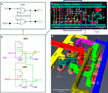
Ptychographic X-ray laminography. A strong disadvantage of the tomography geometry is that the sample has to be accessible to the radiation from a full angular range of 180 degrees. This requires the extraction and mounting of small sample volumes. We recently developed LamNI, an instrument for Laminographic Nano Imaging via ptychography. Here, in contrast to tomography, the axis of rotation is no longer perpendicular to the X-ray beam. The laminography geometry is therefore ideal for imaging extended flat samples, such as integrated circuits. The region of interest can be freely chosen and imaged at various magnification levels. The combination of the state-of-the-art instrumentation, LamNI, and continuous development of reconstruction algorithms a resolution of 18.9 nm was demonstrated in a first experiment, while the imaging volume was increased by a factor 15 compared to the case of tomography, and only limited by the available measurement time.
Besides applicability to integrated circuits these techniques are used to image a broad range of materials including materials science, biology, and energy materials.
The goal of the project is to further increase imaging volume and imaging speed, allowing the technique also to be used at higher dimensionality, for example for in situ or dynamic studies. This requires further advancement of instrumentation and reconstruction techniques, as well as an increased coherent flux from the synchrotron source. Thus, the project will immediately benefit from the planned upgrade of the Swiss Light Source towards a diffraction limited storage ring.
References
High-resolution non-destructive three-dimensional imaging of integrated circuits. M. Holler, M. Guizar-Sicairos, E. Tsai, et al. external pageNature 543, 402–406 (2017).
LamNI – an instrument for X-ray scanning microscopy in laminography geometry. M. Holler, M. Odstrčil, M. Guizar-Sicairos, et al. external pageJ. Synchrotron Rad. 27, 730-736.
Alignment methods for nanotomography with deep subpixel accuracy. M. Odstrčil, M. Holler, J. Raabe, and M. Guizar-Sicairos. external pageOptics Express Vol. 27, Issue 25, pp. 36637-36652 (2019).
external pageThree-dimensional imaging of integrated circuits with macro- to nanoscale zoom. Mirko Holler, Michal Odstrcil, Manuel Guizar-Sicairos, Maxime Lebugle, Elisabeth Müller, Simone Finizio, Gemma Tinti, Christian David, Joshua Zusman, Walter Unglaub, Oliver Bunk, Jörg Raabe, A. F. J. Levi & Gabriel Aeppli external pagehttps://spectrum.ieee.org/chip-x-ray