Van der Waals materials & devices
We investigate the photo- and electrically-induced topologically protected hidden state in the layered transition metal dichalcogenide 1T-TaS2.
Electronic properties of Van der Waals (VdW) materials can be influenced by external parameters such as the stacking order, gating and the twist angle between the sheets. The latter introduces a new moiré superlattice structure in real space along with flat energy bands and a high density of states in reciprocal space which can give rise to collective behavior and exotic ground states. Hence, twisted VdW devices are an ideal platform to engineer quantum many-body states to study strongly correlated physics and topology.
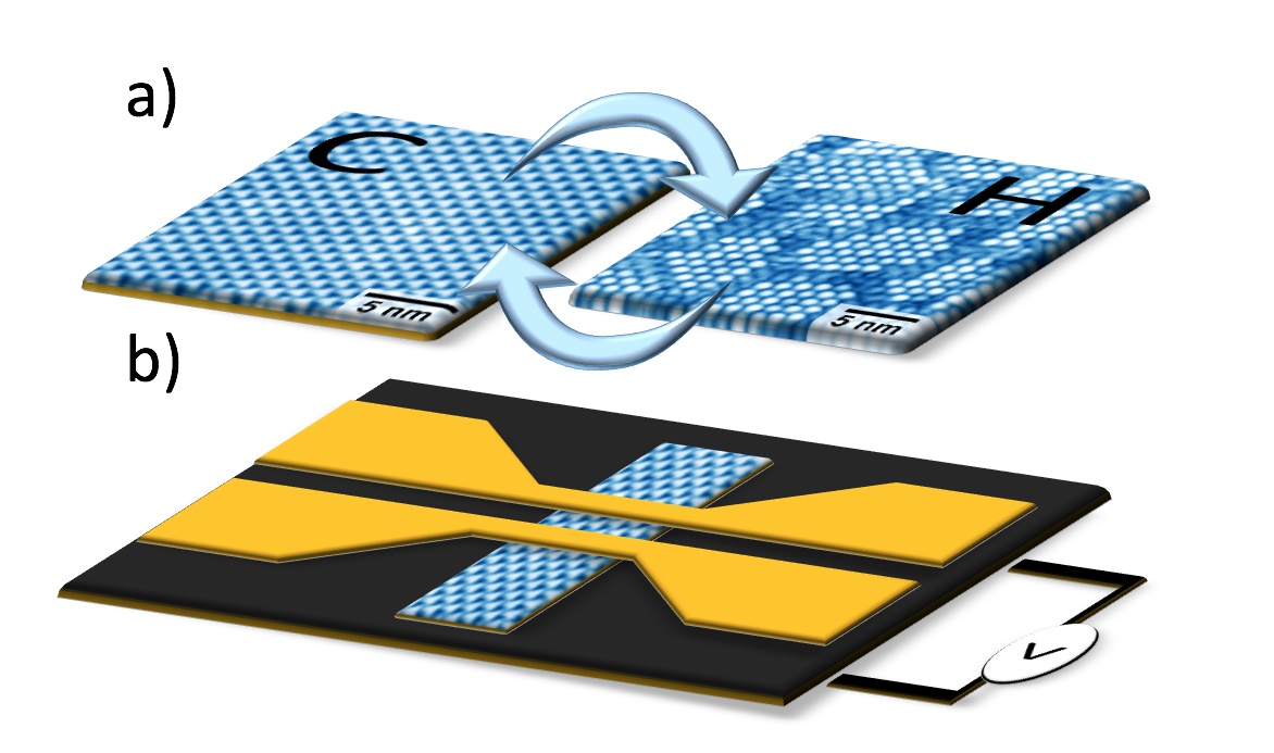
1T-TaS2 is a layered transition metal dichalcogenide, which exhibits a variety of equilibrium states, ranging from metallic at high temperature, a series of charge-density wave (CDW) states at intermediate temperatures and an insulating Mott state below 180 Kelvin. Intriguingly, a variety of long-lived metastable photo- and electrically-induced states are found, which are stable at low temperatures. Combining the knowledge of these equilibrium and non-equilibrium phases with a moiré potential via twisting allows us to increase electron correlations and opens the door to induce new ground states.
In this project, we investigate the photo- and electrically-induced so-called “hidden” state of 1T-TaS2, which has orders of magnitude lower resistivity than the thermodynamically stable insulating low-temperature state. The transition to this photoinduced state occurs on sub-picosecond timescale, making the material an ideal candidate for ultrafast low-energy non-volatile memory devices. We work in collaboration with the external pageJozef Stefan Institute (JSI) where the material is synthesized and characterized using optical methods and scanning tunneling microscopy. For device fabrication, we use PSI’s state-of-the-art external pagecleanroom facilities at PSI and employ synchrotron and X-ray free-electron laser techniques to shine light on the equilibrium and non-equilibrium physics.
Recent Publications
Quantum billiards with correlated electrons confined in triangular transition metal dichalcogenide monolayer nanostructures
J. Ravnik, Y. Vaskivskyi, J. Vodeb, P. Aupič, I. Vaskivskyi, D. Golež, Y. Gerasimenko, V. Kabanov & D. Mihailovic
external pageNature Communications 12, 3793 (2021)
DOI: 10.1038/s41467-021-24073-0.
Charge configuration memory devices: energy efficiency and switching speed
A. Mraz, R. Venturini, D. Svetin, V. Sever, I. A. Mihailovic, I. Vaskivskyi, B. Ambrozic, G. Dražić, M. D’Antuono, D. Stornaiuolo, F. Tafuri, D. Kazazis, J. Ravnik, Y. Ekinci, D. Mihailovic
external pageNano Lett. 22, 4814 (2022)
A time-domain phase diagram of metastable states in a charge ordered quantum material
J. Ravnik, M. Diego, Y. Gerasimenko, Y. Vaskivskyi, I. Vaskivskyi, T. Mertelj, J. Vodeb & D. Mihailovic
external pageNature Communications 12, 2323 (2021)
DOI: 10.1038/s41467-021-22646-7.